Google Search

Friday, June 22, 2012

AMD Radeon HD 7970 GHz Edition Review:Going For The Performance Crown

 NVIDIA launched their GeForce GTX 680 to rave reviews and a boatload of editor recommendations, reclaiming their crown for the fastest single-GPU video card in the process. And for the first time in many years NVIDIA didn’t just beat AMD on raw performance, but they achieved the complete holy trifecta of video card competition – higher gaming performance, lower power consumption, and a lower price.

Consequently, for AMD this launch marked both the closest and the farthest they’ve ever been from outright beating NVIDIA in modern times. On the one hand NVIDIA beat them by more than usual by achieving the holy trifecta as opposed to focusing just on performance. And yet when it comes to raw performance AMD has never been this close. Where the GTX 580 beat the 6970 by 15% the GTX 680 led by just 10%, and even then it lost to the 7970 on some games. With such a close gap an obvious question arises: maybe, just maybe AMD could meet or beat NVIDIA with a higher clocked 7970 and rival them for the performance crown?
Today AMD is putting that idea to the test with the launch of the Radeon HD 7970 GHz Edition. Although AMD is not calling the 7970 GHz Edition a response to the GTX 680 – instead choosing to focus on it being Tahiti’s 6 month birthday – for all intents and purposes this is AMD’s response to the GTX 680. A higher clocked 7970 with AMD’s take on GPU turbo intended to make a run at the GTX 680 and that performance crown.As we’ll see, after today it will no longer be clear who holds the performance crown.
AMD GPU Specification Comparison
AMD Radeon HD 7970 GHz Edition AMD Radeon HD 7970 AMD Radeon HD 7950 AMD Radeon HD 6970
Stream Processors 2048 2048 1792 1536
Texture Units 128 128 112 96
ROPs 32 32 32 32
Core Clock 1000MHz 925MHz 800MHz 880MHz
Boost Clock 1050MHz N/A N/A N/A
Memory Clock 6GHz GDDR5 5.5GHz GDDR5 5GHz GDDR5 5.5GHz GDDR5
Memory Bus Width 384-bit 384-bit 384-bit 256-bit
VRAM 3GB 3GB 3GB 2GB
FP64 1/4 1/4 1/4 1/4
Transistor Count 4.31B 4.31B 4.31B 2.64B
PowerTune Limit 250W+ 250W 200W 250W
Manufacturing Process TSMC 28nm TSMC 28nm TSMC 28nm TSMC 40nm
Architecture GCN GCN GCN VLIW4
Launch Date 06/22/2012 01/09/2012 01/31/2012 12/15/2010
Launch Price $499 $549 $449 $350
As far as performance and functionality goes, the Radeon HD 7970 GHz Edition (7970GE) is a rather straightforward upgrade to the existing Radeon HD 7970. In fact the hardware is absolutely identical right down to the GPU – there have been no changes to the PCB, the cooling, or the VRMs, and even the Tahiti GPU is the same revision that has been shipping in the 7970 since the beginning. Everything the 7970GE adds to the 7970 is accomplished through chip binning and new Catalyst and BIOS features specific to the 7970GE. So in many ways this is the 7970 we’ve already become familiar with, but with more pep in its step.

With identical hardware the real difference is in clockspeeds. The 7970 shipped at a rather conservative 925MHz core, which as we’ve seen in our 7970 overclocking adventures ends up being a good 175MHz less than what our worst 7970 can hit while overclocked without overvolting. At the time AMD left a lot on the table in order to maximize yields and to give their partners headroom to launch a range of factory overclocked cards, and now AMD has come to take that headroom back for themselves.
The 7970GE will ship at 1GHz, 75MHz faster than the 7970. Furthermore the 7970GE introduces AMD’s PowerTune Technology with Boost, which is AMD’s name for GPU turbo, and similar to the GPU turbo feature that is already on AMD’s APUs. The 7970GE can boost a further 50MHz up to 1050MHz, which means the 7970GE’s core clock increase is anywhere between 8% and 13.5% depending on how high it can go under a specific workload. We’ve seen that AMD’s performance scales very well with clockspeeds – which is to say it’s typically not memory bandwidth bottlenecked – so this bodes well for its performance. All the same AMD has also boosted their memory clocks from 5.5GHz to 6GHz, which will give the card 9% more memory bandwidth with it needs it. AMD hasn’t provided any specific guidance for performance, but overall you can expect around 10% better performance over the 7970 in GPU-bound situations, which is exactly what AMD needs to close the GTX 680 gap.
Beyond the higher clockspeeds and introduction of PowerTune Technology with Boost, that sums up the changes for the 7970GE. There are no board changes and it’s the same Tahiti GPU, meaning 2048 stream processors paired with 128 texture units and 32 ROPs, all on a 4.31B transistor GPU with a die size of 365mm2. With the increase in clockspeed from 7970 this pushes AMD’s theoretical double precision  compute performance over 1 TFLOPs to 1.08 TFLOPs, which AMD is in no way shy about mentioning since they’re the first GPU vendor to get there. On the memory side of things, AMD is using the same 3GB of GDDR5 we’ve previously seen, just clocked higher.

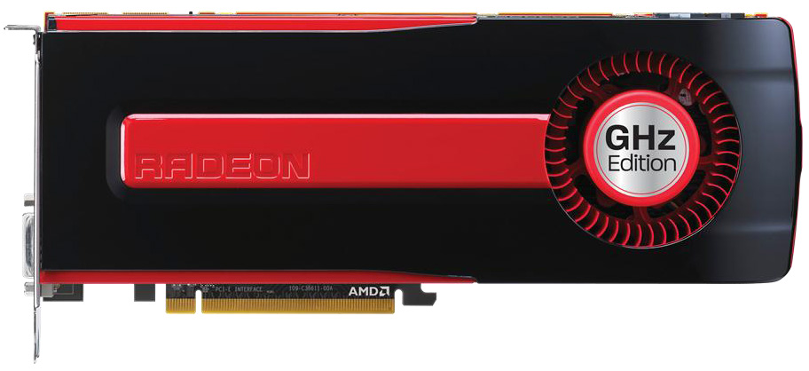
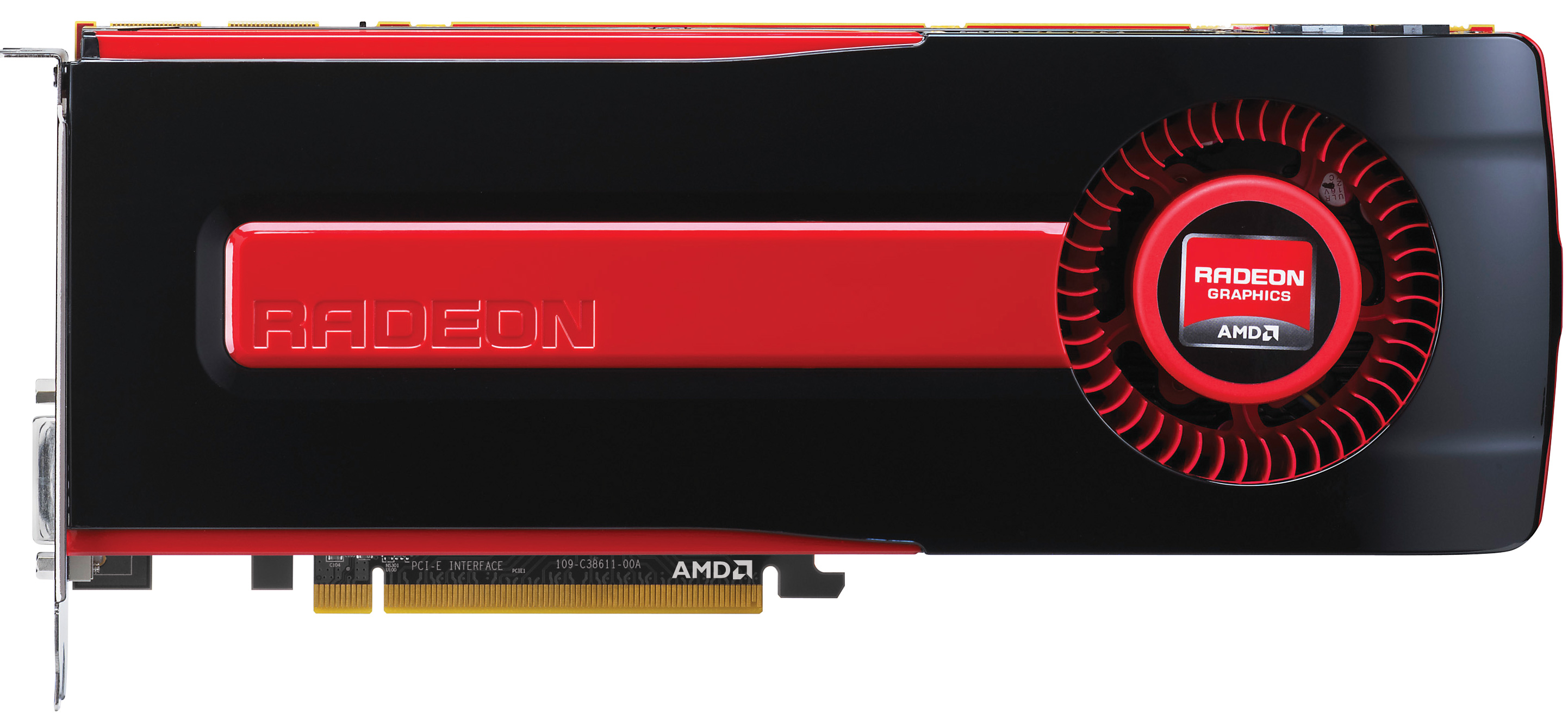
Idential Twins: Radeon HD 7970 GHz Edition & Radeon HD 7970
On that note, because AMD hasn’t made any hardware changes for the 7970GE the 7970GE’s TDP/PowerTune limit is equally unchanged. The 7970GE will have a PowerTune limit of 250W, identical to that of the 7970. With 6 months between the launch of the 7970 and the 7970GE, that’s 6 months of 28nm process improvements over at TSMC, which AMD will be using as the basis of their binning for the 7970GE. With that said there’s no such thing as a free lunch, and in practice the 7970GE’s power consumption has still increased relative to the 7970, as we’ll see in our benchmarks.
On a final point, at this point we would be remiss to not point out that once again AMD has once again added confusion to their product naming system in the name of simplicity. We have always pushed for clear naming schemes where parts with different specifications have different names and for good reason. AMD’s decision to name their new card the 7970 GHz Edition is unfortunate; while it’s true it has the same Tahiti GPU its performance and feature set (PowerTune Boost) are entirely different from the 7970. What’s the point of a 4 digit number if AMD is only ever going to use a fraction of them? In a rational universe this card would be the 7975 and that would be the end of that.
Our primary concern here is that a potential customer is going to read this review and then go out and buy a vanilla 7970 thinking they got the GHz Edition, which is the kind of misleading situation we want product names to avoid. At this point if AMD is going to continue producing multiple products under the name model number – and I can’t believe I’m saying this – they need to bring back proper suffixes. They were less sufferable than “GHz Edition”, which is just long enough to be ignored. At the end of the day clockspeed is not a proper product name.

Anyhow, with clocks and hardware settled, let’s talk about competitive positioning, pricing, and availability. As we alluded to in the introduction, the 7970GE is a clear swipe at the GeForce GTX 680. NVIDIA had a smaller than usual 10% lead with the GTX 680, and as a result AMD is making a run at it with a higher clocked Tahiti part. Realistically speaking, on average AMD can’t beat the GTX 680 with the 7970GE, but with good performance scaling they can tie.
Seeing as how it’s a GTX 680 competitor then, it should come as no surprise that AMD has put the MSRP on the 7970GE at $499, the exact same price as the GTX 680. It’s a slugfest for sure. At the same time it’s no secret that Tahiti cards are relatively expensive to manufacture – thanks to the larger-than-GK104 GPU and 3GB of GDDR5 – so AMD is keen on not just challenging NVIDIA for the crown but also bringing their margins back up to where they were prior to the GTX 680’s launch.
While the price of the 7970 and 7950 aren’t officially changing in the wake of the 7970GE’s launch, the launch of the GTX 600 series has already pushed pricing down to levels below even AMD’s April MSRPs. Reference clocked 7970s are down to around $430 after rebate, and the 7950 (having been pushed out of the picture by the GTX 670) is down to about $360 after rebate. Barring a move from NVIDIA, we expect AMD’s stack to settle here for the time being.
Finally, while general card availability should be good – we’ve already seen that most 7970s can overclock to 7970GE speeds – AMD has pushed the launch out in front of when cards will actually ship. The 7970GE will not appear in stores until next week and widespread availability isn’t expected until July.by ryan smith

Wednesday, June 20, 2012

Microsoft Surface for Windows 8 Pro Intel Core-i Processor; 10.6-display

Microsoft announced its latest Surface tablets--two versions that run on either Windows 8 Pro or Windows Rt. Microsoft is primarily a software company that depends on many partners to use its operating system and productivity applications. With the Surface, the company signals its intent to focus on the tablet market, which is currently dominated by Apple through a single product, the iPad.
The thicker of the two versions announced runs Windows 8 Pro, and utilizes Intel's Ivy Bridge platform. For storage, it has either a 64GB- or 128GB SSD. These specifications make it very similar to Ultrabooks such as the Asus Zenbook.
The big difference is that it's primarily a slate-like device with a touchscreen display, but can also be fitted with a peripheral called a Touch Cover (which doubles as a pressure-sensitive keyboard) to make it more notebook-like. When in use, a kickstand on the back of the Surface allows it to be propped up in landscape orientation. Another accessory, called the Type Cover, is also available--this is thicker and comes with mechanical keys.
The device also supports stylus input, along with the ability to differentiate between a palm and the pen, so that you will be able to rest your palms on the tablet when using it.
The material for the chassis of the Surface is something Microsoft calls Vapor MG. This is a magnesium-alloy that apparently offers good protection and has a "high-quality finish and feel".
Price and availability has not been announced and we'll likely have to wait till the end of the year since that's when the Windows 8 OS will be launched.
Here are some key specifications:byjohanchan

OSWindows 8 Pro
Weight903g
Thickness13.5mm
Screen10.6-inch 1,920 x 1,080-pixel LCD
Storage64GB or 128GB
PortsmicroSDXC, USB 3.0, mini DisplayPort

Nvidia GTX 685 25% More Performance Than GK104

Finally a REAL flagship from Nvidia. However, changed from my previously mentioned performance advantage, new reports show the GTX 685 (GK110) performing only 25% better than the GTX 680 @ 1110 Mhz Turbo (GK104). A highly clocked 7970 @ 1335 Mhz here (clocked 45% higher than current reference 7970s @ 925 Mhz) But apparently, AMD will already have the 8970 on its way shortly after the release ofthe GK110 in Q3 2012. It doesnt look like Nvidia can easily claim the GPU crown with this product

Tuesday, June 12, 2012

EVGA Geforce GTX 680 FTW

EVGA a few weeks after we got the details on the company’s GeForce GTX 680 SC Signature (with and without backplate), EVGA has announced all the information about the GeForce GTX 680 FTW.

Wrapped in what is essentially the same body as the SC Signature, the FTW card sports a base clock of 1110MHz and a boost clock of 1176MHZ, both a slight bump up from the SC Signature’s 1084MHz/1150MHz. The memory clock is the same--6208MHz (effective)--and they both have 2GB of 256-bit GDDR5 memory and memory bandwidth of 198.66GB/s. The FTW has a slightly higher texture fill rate (142GT/s .


While the SC Signature has a 5-phase PWM design, the FTW has an 8-phase PWM.


EVGA GeForce GTX 680 FTW w/backplate

The FTW packs PCI-E 3.0 (16x), DVI-I, DVI-D, HDMI, and DisplayPort, and of course it supports up to four-way SLI. The price tag for all this graphical bounty is $569.99, or you can opt for the 4GB version of the FTW for $629.99.by sethkolaner

Monday, June 11, 2012

EVGA GTX 670 FTW reviewed

we’re hoping the GTX 670 FTW will fare really well when it comes to noise, overclocking and, thanks to the high factory overclock, performance as well. If you’re looking at the picture below and wondering how can this be when EVGA used reference cooling, the trick is that this is reference GTX 680’s cooling. In fact, EVGA also took the reference GTX 680’s PCB as well.
670ftw1
The GPU is overclocked from reference 915MHz to 1006MHz, while the memory is up from reference 1502MHz to 1552MHz (6208MHz effectively).
gpuz
GTX 670 and GTX 680 graphics cards use the GK104 GPU. EVGA set the GTX 670 FTW’s clocks at 1006MHz, which is the reference clock on the GTX 680. Naturally, performance can’t be the same because the GTX 670 comes with one SMX unit less. This means that the GTX 670 has 1344 CUDA cores while the GTX 680 has 1536 CUDA cores.
Both the GTX 670 and GTX 680 feature identical memory subsystems, packing four 64-bit memory controllers and 2GB of GDDR5. As we already said, EVGA’s GTX 670 FTW comes factory overclocked.
EVGA GTX 670 FTW’s packaging is more or less standard. EVGA ships a large poster and a badge with the card. The rest of the contents are listed below.
In the box you’ll find:
User Guide
Quick Installation Guide
Driver DVD
A small note about PCIE 3 compatibility
A new sticker set (Enthusiast Built)
EVGA Ful Size Poster
EVGA Case Badge
DVI to VGA Dongle
2x Molex to 6-pin Power Adapter
in-the-box


Nvidia uses a shorter PCB in order to cut costs, but EVGA didn’t want to skimp here so the company threw in the GTX 680’s PCB and cooling solutions. Note that doing this was not very difficult since both the GTX 680 and GTX 670 use the GK104 GPU and identical memory subsystems.

670ftw
670ftw1

GTX 670’s reference cooling did really well when it comes to performance and noise. The fan is not very loud and working next to a GTX 670 under full load is quite comfortable. Still, reference cooling turns loud quickly once the GPU is overclocked. EVGA GTX 670 FTW’s GPU is overclocked by 91MHz (1006MHz), something which would be too much for the reference cooler to remain silent. However, EVGA ended up using a cooler that did great on performance and noise tests, which we will cover in more detail later on.

GTX 670 FTW is 25,4cm long, just like the GTX 680, while the reference GTX 670 is 24cm long. Although the actual difference in size of GTX 670 and GTX 680 is negligible, their PCBs are in fact sized differently. The difference is 8.2cm. The picture below first shows the GTX 670 FTW, followed by the GTX 670 Superclocked.
670-ftw-cooler
670-ftw-back
570-heatsink-3

670-power
EVGA’s GTX 670 FTW packs a total of 2GB of GDDR5, in eight memory modules. EVGA used Hynix memory chips (model No: H5GQ2H24AFR-R0C), which are specified to run at 1500MHz (6000MHz GDDR5 effectively). EVGA overclocked the memory to 1552MHz (6208MHz effectively).

EVGA’s GTX 670 FTW draws power via two 6-pin power connectors, just like the reference version of the card. Thanks to GTX 680’s PCB, EVGA’s GTX 670 FTW offers superior TDP settings changes (all the way up to +145 percent)
670-ftw-cooler2
Back when we were testing the GTX 670 Superclocked, we thought EVGA’s backplate would come in pretty handy. Unfortunately, we weren’t granted the wish with the GTX 670 FTW. In case you want it, you’ll have order the GTX 680’s backplate. Naturally, this is not something that you must have, but it does look nice.
680 BackPlate
The I/O panel has two dual-link DVIs, one HDMI and one Display Port. DVI-to-VGA dongle can only be used on the DVI-I out. The protective caps are quite a nice touch. GTX 680/670 graphics card can run four displays at the same time.


crysis2


avp1

it’s clear that EVGA’s GTX 670 For The Win is in fact a winner. The factory overclock ensured that the card scores really close to the GTX 680, which is quite appealing, especially after considering the difference in price. When buying any graphics card, especially the factory overclocked cards, we usually look at the cooling first. In many cases you’ll get higher clocks and improved performance at the expense of silence. This is not the case with EVGA’s GTX 670 FTW, which remains silent in pretty much any scenario.
The GTX 670 FTW is priced at about $420,Considering the silence and a high factory overclock, we could say it’s worth it. Gaming performance of the GTX 670 is hardly worth discussing any more, since they are among the fastest graphics cards on the market. Since availability of GTX 680 cards is yet to become healthy, those waiting for one may find EVGA’s GTX 670 For The Win to be a worthy alternative, if not replacement.bysanjinrados

Sunday, June 10, 2012

Nvidia GeForce Kepler GPU architecture explained


High above the sun-baked streets of San Francisco, in a hotel bar - which bears more than a passing resemblance to the Emperor's throne room on the unfinished Death Star - I find myself talking to a vice president at Nvidia.
When challenged that Kepler was essentially just a die-shrink of the Fermi architecture, his reaction was not the one I expected. The amount of alcohol imbibed by us both may have had something to do with the vehemence with which he countered the argument. Suffice to say, he referred to the previous generation in less than glowing terms - derogatory terms that probably shouldn't find their way onto a site as innocent or polite as TechRadar.
He's right though; while there are definite similarities to the last Nvidia graphics technology, Kepler is still a different beast to Fermi, and is much more than just the actual hardware too. But lets cover that die-shrink first.

Like AMD, Nvidia has taken the plunge and chosen a 28nm production process for this generation of its graphics cards. That means that, compared with the GTX 580, this new GTX 680 can achieve a far smaller die size and still manage to cram in more transistors than ever before.
We're talking about the GTX 680's GK104 GPU as a 295mm2 chip, compared with the 520mm2 GF110 in the GTX 580. That's a smaller chip than the GTX 560, with another 500 million transistors more than the GTX 580. It's also a far smaller chip than AMD's 28nm Tahiti GPU at 352mm2, although AMD is claiming to have packed over an extra billion transistors into its top-end chip.
From those simple figures, you could easily infer that the Nvidia architecture is considerably less power-hungry than either its predecessor or the competition, and you'd be right. The GTX 680 is actually a sub-200w card, operating at its base clock of 1,006MHz at 195W under full load, while the GTX 580 and HD 7970 are 244W and 230W cards respectively.

So many shaders...


Those numbers might look impressive on the surface, but what's actually going on inside and why are we now talking about a GPU's base clock as if it were a CPU?
Despite the ever-bombastic Gearbox CEO Randy Pitchford referring to it as 'a simulation CPU' because of the advanced PhysX and Apex effects, this is still very much a gamer's GPU. But Nvidia has taken more than a leaf out of Intel's book - more on that later.
First of all, let's take a look at the make up of the GK104 GPU. Like Fermi, the Kepler GPU is made up of multiple CUDA cores jammed into multiple Streaming Microprocessors . These SMs act like simple processors, each concurrently taking on an action, making for impressive parallelism a cornerstone of GP-GPU computing.
But these are no longer called plain ol' SMs. Oh no, they're now called SMXs, which by today's nomenclature probably stands for Streaming Microprocessor Xtreme. But compared with the old SMs of the Fermi days, they could easily be deemed 'Xtreme'.
Previously each contained a total of 32 CUDA cores; in Kepler that figure stands at a whopping 192. Even with half the SM blocks of the GTX 580, you're still looking at 1,536 CUDA cores/shaders spread out over 8 SMXs.
Nvidia is claiming a 2x improvement in terms of performance/watt compared with the GTX 580. That figure seems a little conservative considering the GTX 680 comes with three times the CUDA cores, but while they are physically identical to the cores in the Fermi architecture, they are clocked much slower. In fact, they're half as fast because Nvidia has decided not to have a separate shader clock. Instead we have one solitary base clock covering everything.

Boostin'

And there it is again - that base clock. For every Kepler-based graphics card we're now going to be quoting two separate frequencies; one is the base clock and the second is the Boost clock.
Nvidia has been totally honest and admitted that it copied the idea from Intel - that it's "standing on the shoulders of a great company," as Drew Henry, general manager of GeForce's desktop unit puts it. So we now have Turbo Boost for GPUs - the snappily titled GPU Boost.
In previous GPU generations, the final clockspeed was determined by the worst-case scenario of the application power usage, which meant typically taking the most power-hungry app around and setting the clockspeed to match that power draw. But the draw on the GPU varies massively between different programs. Just taking Fermi as an example, the power required for apps could vary by as much as 50 per cent, so on lower-powered apps there's a lot of GPU headroom not being used.
GPU Boost analyses the amount of power an application is using and boosts the GPU frequency with the amount of extra headroom it has at its disposal. It's also completely application independent - you won't need a new Kepler profile when a game gets released to take advantage of GPU Boost - it's all based on measurements coming directly from the GPU's sensors in real time. Kepler can dynamically alter its clock and voltage every 100ms; essentially every few frames the GPU has a decision to make on clocks and voltage settings.
Since this is just the first generation of GPU Boost, you can expect that to be done more quickly over time. This auto-overclocking doesn't mean an end for traditional overclocking though. "GPU Boost is like overclocking's little buddy… our GTX 680 is a monster overclocker," says Tom Petersen, Nvidia
bydavejames

Friday, June 8, 2012

Evga Geforce GT 640


Core Specs

  • 384 CUDA Cores
  • GPU Clock: 901 MHz
  • Bus: PCI-E 3.01
  • Texture Fill Rate: 28.8 GT/s

Memory Specs

  • Memory Detail: 2048 MB DDR3
  • Memory Bit Width: 128 Bit
  • Memory Clock: 1782 MHz
  • Memory Bandwidth: 28.5 GB/sec

Key Features

  • NVIDIA SMX Engine
  • NVIDIA Adaptive Vertical Sync
  • NVIDIA Surround
  • Supports three concurrent displays; two dual-link DVI connectors, one Mini HDMI
  • Microsoft DirectX 11 with Direct Compute 5.0 support
  • NVIDIA PhysX Technology
  • NVIDIA 3D Vision Ready**
  • NVIDIA CUDA Technology
  • PCI Express 3.0 Support
  • OpenGL 4.2 Support
  • OpenCL Support